From a discarded panel to a certified wafer.

Four stages, twelve partners, one continuous chain. Nothing is handed off to a step outside the consortium.

From a discarded panel to a certified wafer, inside one consortium.

Four stages. Each one names what enters it, what happens inside, and what leaves.

Enters · Secondary raw materials

End-of-life photovoltaic panels, asbestos mining residues and geothermal water residues, sourced across partner countries.

Happens

COMET leads sourcing and mechanical recovery. Recma improves the efficiency, safety and ergonomics of panel dismantling, investigating automatic size detection, assisted carrying and automated aluminium collection.

Leaves

Separated glass, silicon and metal fractions, plus silica-bearing residues, with projected volumes assessed across partner countries.

Enters · Purification

Recovered fractions and silica-bearing residues from stage one.

Happens

Université de Sherbrooke produces high-purity silica from asbestos residues. NTUA optimises purification of precipitated geothermal silica. Kore Metals validates silicon metal at 3–4N. NTNU applies aluminothermic reduction to reach metallurgical-grade silicon.

Leaves

Semiconductor-bound feedstocks: high-purity silica, metallurgical-grade silicon, recovered antimony and silver.

Enters · Ingoting & wafering

Purified silicon feedstock and recovered antimony.

Happens

IKZ Berlin runs Czochralski crystal growth and wafering for silicon and indium antimonide, developing magnetic-field approaches to reduce oxygen and carbon impurities. Topsil GlobalWafers contributes float-zone expertise and wafers the ingots.

Leaves

Crystals and wafers evaluated against the requirements of the power semiconductor market.

Enters · Qualification, security & LCA

Wafers, and samples drawn from every preceding step.

Happens

CSEM develops surface passivation and characterisation for ultra-high-quality electronic-grade wafers, plus authentication and traceability methods, and leads environmental and social life cycle assessment. Advanced Isotopic Analysis applies isotopic analysis across the chain. PowerShift carries the results into policy.

Leaves

Qualified electronic-grade material with a verifiable provenance record and an assessed environmental and social footprint.

Three materials, three routes.

Every gram WISER recovers has a documented origin. These are the routes the consortium is building.

Sb 51

Antimony

Antimony enters the chain inside the glass of end-of-life photovoltaic panels, where it was originally added as a fining agent. COMET and NTNU co-develop the hydrometallurgical process that separates it from the glass matrix and validate it at pilot scale.

IKZ Berlin then grows the recovered antimony into indium antimonide crystals — a compound semiconductor used in infrared detection and high-speed electronics.

PV panel glass Hydrometallurgical extraction InSb crystal

Si 14

Silicon

Silicon reaches WISER by three separate roads. Université de Sherbrooke recovers high-purity silica from asbestos mining residues at above 99 % purity. NTUA purifies precipitated silica from geothermal resources. Kore Metals validates a low-carbon electrochemical route to silicon metal at 3–4N from secondary raw materials including recycled glass.

NTNU reduces the refined feedstocks to metallurgical-grade silicon by aluminothermic reduction. IKZ Berlin grows Czochralski crystals — using magnetic fields to suppress oxygen and carbon impurities — and Topsil GlobalWafers takes ingots through to wafers for power semiconductor applications.

PV wafers & glass Asbestos residues Geothermal silica Purification Ingot & wafer

Ag 47

Silver

Silver sits in the metallisation printed onto photovoltaic cells. COMET and NTNU co-develop the hydrometallurgical process that extracts it from the silicon fraction, and validate the result at pilot scale.

It is a contact metal the semiconductor industry depends on, and one that is currently written off when panels are recycled for their glass and aluminium alone.

PV cell silicon Hydrometallurgical extraction Recovered silver
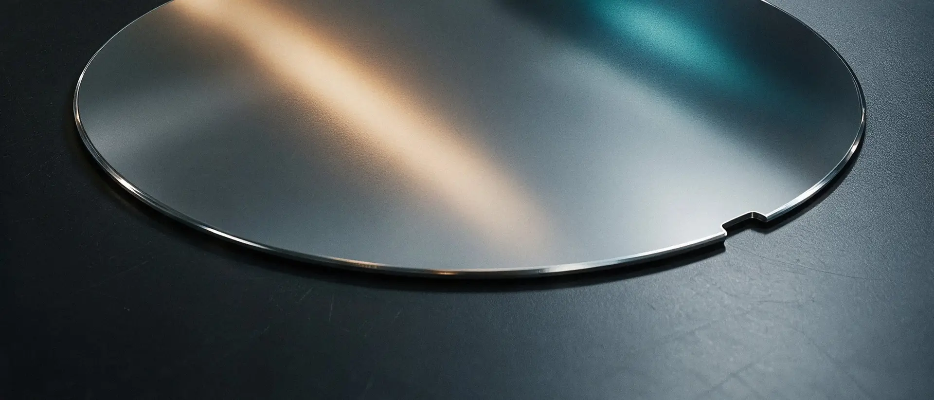
A bare mirror-polished monocrystalline silicon wafer on a dark laboratory bench, its alignment notch visible on the rim

This is the end of the chain.

Not a recovered powder with a purity certificate — an electronic-grade wafer, evaluated against the requirements of the power semiconductor market. Illustrative image.

A fingerprint the material carries itself.

Recovered material only counts if a buyer can prove where it came from. WISER’s answer is not a label or a database entry — it is a signature inherent to the material.

Sample at source

Advanced Isotopic Analysis applies non-traditional isotope and elemental analysis to key samples across the value chain, from raw to processed material.

Follow it through processing

The signature is tracked as material moves through recovery, purification and crystal growth, so a change of origin cannot pass unnoticed.

Certify the wafer

CSEM’s authentication and traceability methods tie qualified material back to its verified secondary source — supporting traceability and anti-counterfeiting for the semiconductor industry.

Who does what.

Twelve partners across ten countries, each with a defined place in the chain.